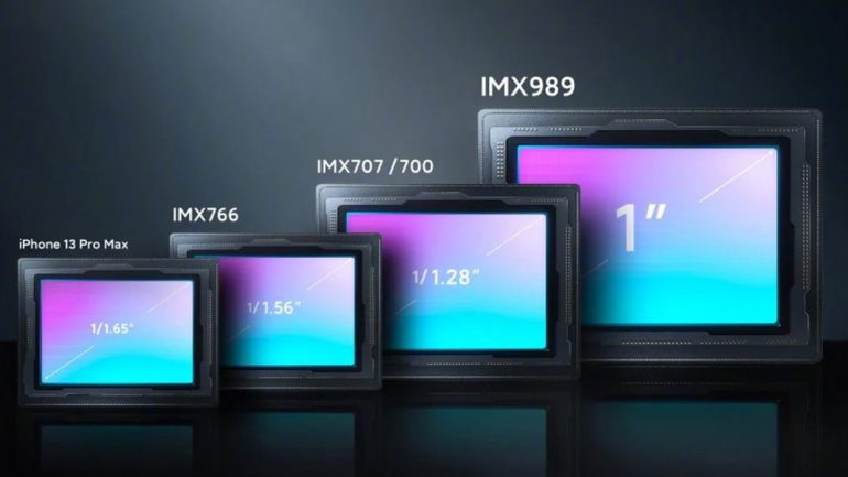
According to a report from ETNews, Sony is looking to move its semiconductor packaging and inspection for its camera sensors in South Korea with Samsung Electronics in mind.
Sony Moves to South Korea to Aid Samsung
The report mentions that Sony Semiconductor Solutions, a subsidiary in charge of making the camera sensors, has plans to move part of its camera sensor production from Japan to South Korea. This is reportedly to help Samsung Electronics expand and strengthen its sensor supply.
The Sony subsidiary is said to have discussed specific cooperation plans with companies that deal with semiconductor post-processing. Among these include LB Semicon, ELT, and Doosan Tesna (Enzion) are among those being targeted.
The packaging processes of the camera image sensor semiconductor wafer will be transferred to South Korea. The Japanese company requested the South Korean firms to use Class 10-level Clean Rooms for the post-processing. These are rooms in a facility with less than 10 dust particles in one cubic foot of space.

This move will reportedly allow Samsung to use more camera sensors from the Japanese company for its smartphones in the future.
Ram found his love and appreciation for writing in 2015 having started in the gaming and esports sphere for GG Network. He would then transition to focus more on the world of tech which has also began his journey into learning more about this world. That said though, he still has the mentality of "as long as it works" for his personal gadgets.


